Superjunction MDmesh


Leading the investment and research in the semiconductor field
A distinguishing feature of ST in the silicon chip industry is its continued research and investment in all the principal categories of power semiconductor products. These include silicon-based MOSFET and insulated gate bipolar transistors (IGBT), as well as silicon carbide (SiC) and gallium nitride (GaN) products based on wide-bandgap (WBG) materials.
Conventional planar architecture
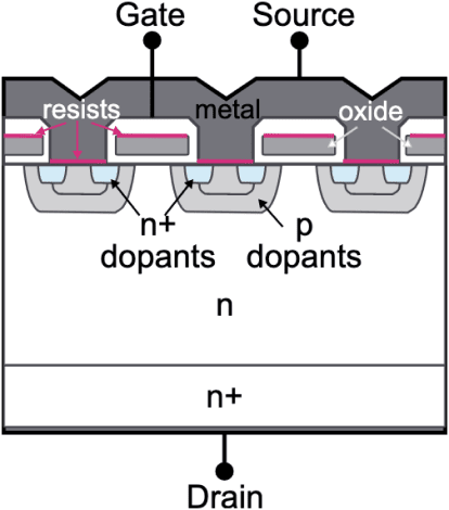
The first power MOSFET devices in planar technology were introduced in the 1970’s. The manufacture of planar MOSFETs involves several processes with various applications of oxides, impurities, and resists to derive the final product.
Planar manufacturing steps:
- oxide film applied to wafer
- p-layer dopants implanted on surface and heat treatment disperses into the wafer
- resists applied
- n+ dopants implanted on surface and heat treatment disperses into the wafer
- resists removed

On-resistance limits in planar architecture

In conventional, high-voltage planar MOSFETs, the blocking or drain to source breakdown voltages (V(BR)DSS) are a function of thickness and doping. There is a direct relationship between blocking voltage and drain to source on-resistance (RDS(on)) and there is a physical limit beyond which RDS(on) cannot be lower.
When a voltage is applied, the depletion region or drift layer expands, which generates the drain to source voltage. As the concentration of the impurity in the drift layer cannot be increased, a high voltage MOSFET requires a relatively thick drift layer, which leads to a high RDS(on). The relationship between the blocking voltage and on-resistance in conventional, high-voltage planar MOSFETs is expressed as: V(BR)DSS2.5∞RDS(on)
Superjunction architecture
Superjunction MOSFETs overcome the limits of planar design with deep, narrow trenches etched into the wafer. This architecture significantly reduces the growth of the depletion region, which allows for a greater concentration of impurities and consequent reduction in RDS(on).


Maxwell’s equations state that the slope of the electric field is equal to the charge density r divided by permittivity e: 
The voltage V is the integral of E, or the shaded area under the E curve as a function of y. Comparing the graphs, the introduction of the p-type pillar significantly alters the electric field distribution and increases the voltage that can be sustained at the OFF state. For a given voltage, we can therefore reduce drain resistivity and thereby lower on-resistance.
MDmesh superjunction technology by ST
The trademark MDmesh MOSFET line represents two decades of concerted development in vertical structures and horizontal layouts, leading to market leadership across various features, including the critical RDS(on) x area.
The earlier series MDmesh MOSFETs represent very mature technologies covering full ranges of cost-competitive devices. More recent series offer significant performance and efficiency gains under specific operating conditions, circuit topologies, and voltage ranges. The MDmesh M6 series, for example, offers greater performance in resonant converters than the preceding MDmesh M2 series.


Superjunction fast recovery power MOSFETs
The evolution of MDmesh transistors is delivering ongoing improvements across a growing range of power conversion applications. One such evolution is the introduction of lifetime killing techniques like platinum ion implantation to enhance the performance of the integral body-diode. The improvements in terms of reverse recovery time, reverse recovery charge and dV/dt (DM series) offer significant application benefits in bridge and high-power phase-shift circuits.


MDmesh state of the art
MDmesh technology continues to target higher power densities for more compact market solutions. The latest iteration of ST superjunction technology is ideal for hard-switching and resonant topologies in high-power-density systems.
This new MDmesh M9 series features:
- best RDS(on) x area
- significant hard- and soft-switching performance improvement
- DM9 FAST diode embedded version
- higher power and greater efficiency
- increases power density
- improves system ruggedness
- better electrical parameters
The latest very-high-voltage series launched in July 2022 has established new best-in-class levels of performance and efficiency.
This new MDmesh K6 series features:
- best RDS(on) x area
- increases power density
- lower threshold voltage
- lower total gate charge Qg
Development for present and future applications
Superjunction MDmesh development is guided by performance criteria in specific applications and the broad demand for higher power density.
Telecom server
MDmesh development supports telecom server and 5G base station size reduction through more compact and efficient power supplies, very high-volume production capability, and cost- competitive performance.


Automotive
HV MDmesh power MOSFETs are being optimized to meet the requirements for electric vehicle applications, including on-board chargers, HV-LV DC-DC converters, and auxiliary power supplies in compliance with stringent automotive quality standards.


Power supplies
With the broad transition to LED lighting technology in urban, industrial, and domestic contexts, there is significant focus on efficient power supplies. MDmesh development targets compactness across wide load ranges for LED drivers using power MOSFETs both in flyback and efficient topologies.


Solar inverters
Solar inverters typically involved high power systems requiring switches with high current ratings. The current trend to distributed networks with microinverters for individual panels is driving the development of MDmesh products tailored for resonant topologies in highly compact packages.

