 |

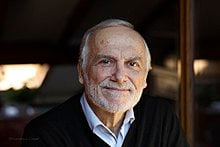 | Giulio Pozzi Giulio Pozzi was born in Riva del Garda in 1945, he received the degree in physics in 1968. He was professor in Bologna University in the Physics department. He is author with Pier Giorgio Merli and Gianfranco Missiroli of the double slit experiment with single electrons. His research activity is focused mainly on the development of electron microscopy applied to the study of magnetic and electric fields. He gave a significant contribution to the birth of a research line on interferometry and electronic holography and has collaborated with the major national and international research centres. He published over one hundred scientific articles in Italian and international journals. He retired from teaching in 2011, but continued his activity as Alma Mater Professor in the Physics and Astronomy Department of the University of Bologna until 31st October 2017. He is co-author of the documentary "L’esperimento più bello" (2011) which won an award at the Brussels Movie Festival in 1976. |
 | Simona Boninelli S. Boninelli obtained the Ph.D. in Physics (cum laude) at the University of Catania (Italy) in 2005. Afterwards, she had a two years postdoc fellowship at the institute CEMES-CNRS in Toulouse (France). From 2008 to 2009 she has been "Team Leader" at the Italian Institute of Technology in Genoa (Italy). In 2007 she received the Young Researcher Award from Accademia Gioenia of Catania (Italy). Nowadays she is Staff Scientist at IMM-CNR Catania, as responsible of the Electron Microscopy laboratory. Since 2012 she has been engaged to perform frontal and practical lessons devoted to master and post-graduated students on Nanostructure Characterization by Transmission Electron Microscopy. She has been tutor of 5 master and a PhD thesis in Physics and responsible of fellowship. Her research activity is devoted to the comprehension of the structural properties of Si, SiC and Ge-based thin films and nanostructured materials. She is co-author of about 90 scientific papers, 4 chapters of books dedicated to silicon microphotonics and editor of two thematic series (Beilstein Journal of nanotechnology and Physica Status Solidi a). Her h-index is 24 (source: Google Scholar). Since 2016 she has been general chair of the 6th and 7th International Conference on Nanostructures and Nanomaterials Self-assembly (NanoSEA) and two EMRS symposia. |
 | Vittorio Morandi Vittorio Morandi, Senior Scientist at CNR-IMM, graduated and obtained the PhD in Physics at University of Bologna in 2003. He is author of more than 100 papers in high impact international journals, with more than 3000 citations and H-index 26 (source Google Scholar). He has participated to about 40 international conferences with oral presentations, with talks on SEM, STEM, graphene characterization and exploitation. Since 2005 he has been supervisor of eight master degree students and three PhD students of University of Bologna, Parma and Roma “La Sapienza”, in physics, chemistry and electronic engineering. He is presently Head of the Bologna Section of IMM-CNR and Coordinator of the Graphene Technology Group at IMM-CNR in Bologna, and member of the team of the Beyond Nano Electron Microscopy Lab (http://www.beyondnano.it), one of the largest facilities on Transmission Electron Microscopy in Italy. He has been the chairman of GraphITA 2011 and 2015 (http://graphita.bo.imm.cnr.it), an International Workshop on Synthesis, Characterization and Technological Exploitation of Graphene and 2D Materials Beyond Graphene. Since 2005 he has been teacher in several Electron Microscopy Schools co-organized by the Italian Society of Microscopy Science (SISM http://www.sism.it) giving lectures mainly on Electron-Matter Interaction, Monte Carlo Methods, Scanning Electron Microscopy and Scanning Transmission Electron Microscopy Methods. Since 2005 is one of the organizers of the biannual Transmission Electron Microscopy in Material Science School held at IMM-CNR in Bologna (http://temschool.bo.imm.cnr.it). Since 2010 he is involved in the organization and in the dissemination activities of the project SperimEstate (http://sperimestate.bo.imm.cnr.it), involving nowadays more than 60 high school students in summer laboratory stages in several CNR laboratories in Bologna. |
 | Michele Nacucchi Michele Nacucchi is currently researcher at the Brindisi Research Centre of the Italian National Agency for New Technologies, Energy and Sustainable Economic Development (ENEA). Since April 2010 to June 2015 he was head of the Laboratory “Composites and Nanostructured Materials” of that Centre. Since 1990 he has began to develop expertise in the advanced materials field, specifically focusing on micro-analytical characterization of materials using probes of collimated beams of electrons or X-rays. In 1993 he has become member of the European Society of Microanalysis (EMAS). Due to this expertise, since 1998 Nacucchi is Italian representative in the Technical Committee ISO/TC-202 "Standardisation in the field of microbeam analysis" as an expert in the subcommittee "Electron Probe microanalysis". More recently, he was responsible for ENEA activities in the Apulian regional project, "Materials and methods for innovative products in the field of renewable energy." In this project, he was involved in the measurement of the aging degradation of the mechanical properties of bonded joints of fibre-reinforced plastic material, used in the blades manufacturing of small wind turbines. Since January 2014 he deals with non destructive analyses by high-resolution X-ray computed tomography of different materials, primarily for aerospace applications and bioengineering. The current topic of interest concerns the measurement of spatial anisotropy directly in 3D of cellular and composite materials. |
| Marilena Re Marilena Re. Physicist, since 1991 has been working in the field of Materials Science at the beginning with a fellowship at the C.N.R.S.M (National Centre for Research and Development of Materials) and some periods at CNR-IMM institute (ex LAMEL) in Bologna and at the “Max-Planck Instut für Metallforschung” in Stuttgart. Since 2001 she is a researcher of ENEA, and now she is affiliated with the Department of Territorial and Production Systems Sustainability. An important part of her research activity has been devoted to microstructural and micro-analytical characterization of nanomaterials, polymeric nanocomposites, nanostructures by means of Transmission Electron Microscopy techniques. Since 2013 she has been involved in the characterization and the study of nanomaterials by Helium Ion Beam Microscopy. Currently her scientific activity is focused on electrodeposition and electrochemical characterization of innovative materials, in particular promising as supercapacitor electrodes. In 2003 she was a teacher and a director of the Theoretical and Practical School in Transmission Electron Microscopy in Materials Science, co-organized by the Italian Society of Microscopy Science. She is a co-author of many scientific papers, published in international journals with the referee system, and of communications at national and international conferences, and is referee for some scientific international journals. |
 | Domenico Mello Domenico Mello was born in Brindisi in 1970. He received the degree in Physics from University of Lecce in 1996, discussing research thesis on transmission electron microscopy. In 2001 he received the Ph.D degree in materials science discussing a thesis in surface analysis and ion implantation. In 2000, he joined STMicroelectronics, Catania, Italy, in Process Eng. Group and the year after he moved in QA Lab group. Since 2016 he lead the Physics Laboratory Group which is the laboratory of Catania manufacturing department. Since 1998 he has began to develop expertise in the characterization field of the advanced materials, specifically focusing on micro-analytical and advanced failure analysis of microelectronic materials using electron microscopy and surface analysis methodology. His activity is mainly focused on chemical and morphological characterization in order to ensure the best performances in terms of Quality and Reliability of manufactured products and technologies. He is member of ST technical staff and he is author of many scientific papers, published in international journals with the referee system, communications at national and international conferences, and he is referee for some scientific international journals. |
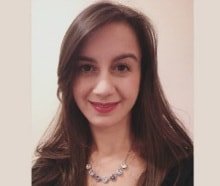 | Marta Agati M. Agati obtained her master degree in Physics at the University of Catania (Italy) in 2013 and hence her Ph.D. in Physics (cum laude) at the University of Catania (Italy) in 2017. The Ph.D. project was conducted in the framework of a cotutelle agreement between the University of Catania and the INRS-EMT (Varennes, Canada), under the supervision of Dr. Simona Boninelli (CNR-IMM, Catania) and Prof. M. A. El Khakani (INRS-EMT). The objective of this project concerned the investigation of Silicon nanowires synthesized by an Inductively Coupled Plasma process, already developed by the Tekna Plasma System Inc. (Sherbrooke, Canada) for the large scale production of nanostructures at the industrial level. Her role was mainly focused on the study of the structural and chemical properties of the Silicon nanowires at the nanoscale level by means of transmission electron microscopy (TEM) techniques. She also performed the chemical characterizations by means of Fourier-transform infrared spectroscopy and she was involved in the optoelectronic characterizations accomplished via photoluminescence measurements. Since 2017 she has been engaged as a postdoc fellow at CEMES in Toulouse (France), under the supervision of Prof. A. Claverie. Here, in the contest of a collaborative project which involves the CEMES, the LPCNO (Toulouse) and ST-Microelectronic (Crolles), her role mainly aims at the understanding of the phase change transition of Ge-rich GeSbTe alloys for memory device applications by means of TEM studies. She presented her results in numerous international conferences and is co-author of 3 scientific papers as well as 1 conference proceeding. |
 | Roberto Balboni Dr., Researcher. He received the degree in Physics at University of Bologna. From 2001 he is researcher at CNR – IMM Institute in Bologna. His areas of interest cover the field of structural and analytical characterization by means of Scanning and Transmission Electron Microscopy and X-ray microanalysis mostly applied to the analysis of semiconductor materials and devices for microelectronics. He also worked on X-ray diffraction characterization and modeling in semiconductor and on electromigration effects in metal interconnects. He participated to the project STREAM (FP5), funded by the Europen Commission (EC) and coordinated by CNR-IMM Bologna, to develop the procedure and codes for strain analysis in semiconductor structures and devices. He was responsible for the CNR participation in the project ANNA (European Integrated Activity of Excellence and Networking for Nano and Micro-Electronics Analysis), funded by the EC. He authored more than 90 papers in international journals and presented his work on more than 70 international conferences. He was Director of the Electron Microscopy School in Materials Science from 2008 to 2016. He is Vice-President of the Italian Society for Microscopical Sciences since 2007. He is presently responsible for the Characterization Department at CNR-IMM Bologna. |
 | Mario Scuderi Mario Scuderi received the Ph.D. degree in physics from the University of Catania (IT) in 2008. Initially his resarch activity concerned astropartichle physics until in 2012 he got a postdoctoral fellow at IMM-CNR to work as trasmission electron microscopist on the Beyond Nano Project. He is currently working at IMM-CNR Catania in the field of materials science. During his activity he conducted research at the Pierre Auger Observatory - Malargue (AR), at the Institute of Theoretical Physics - Wuerzburg (DE) and at the Physics Department of Naples University (IT). He was adjunct professor and got some teaching assignments at the University of Catania. Mario Scuderi is author of more than 100 scientific international papers, his current H-index is 33, with an overall of more than 7700 citations. His research activities mainly concern: Si-Ge nano-structures for micro and nano-electronics, III-V semiconductors, nanomaterials for plasmonic applications, TiO2 based materials, perovskite oxides and chalcogenide materials for PCRAM. |
| Nicolas Bernier Nicolas Bernier got his Ph.D in physics at the University of Marseille, France in 2007. He worked on the study of carbon materials by TEM and EELS to understand the fuel retention in tokamaks for CEA Cadarache. After a post-doctoral position at CEA Grenoble on the TEM analysis of carbon natotubes, he joined the R&D center of ArcorMittal in Ghent (Belgium) as a research engineer. He published five articles as a first author mostly dealing with advanced TEM and EBSD analyses of different steel grades. In 2013, he came back at CEA Grenoble as a TEM specialist. He now focuses on advanced TEM tools (EELS, EDS, strain by precession electron diffraction) applied to semiconductor devices. |
 | Peter Gnauck Carl Zeiss NTS GmbH. Oberkochen, Germany. Peter Gnauck recieved his PhD from the Eberhard Karls University, Faculty of Phyiscs in 2000. From 1995 - 1999 he worked as a research scientist at the NMI (Natural and Medical Science Institute) in Reutlingen, Germany. From 1999 - 2001 he was Project Manager in the R+D department at Carl Zeiss NTS , Oberkochen Germany. During 2001 and 2006 he worked as Product Manager for Focused Ion Beam systems at Carl Zeiss NTS.Since 2006 He holds the position of Senior Business Development Manager at Carl Zeiss Microscopy. |
 | Santiago Sevillano Santiago Sevillano got a Master Degree in Chemistry at University of Salamanca (Spain) in 2002. Started his science carrier in La Rochelle (France) working in a QC Laboratory analyzing GMO´s (Genetically Modified Organisms) and later in the Flychip Facility (Genetics Department) at the University of Cambridge (UK) from 2004 to 2005. In 2007 decided to move into Marketing and Sales working for companies like ISS and VWR-International and finally, since 2011 is working for Leica Microsystems as EM Sample Preparation Specialist for South Europe. At present he is Sales Manager for Western & South Europe at LNT Nanotechnology Division. |
 | Rostislav Vana Rostislav Vana is Head of R&D Applications department. He is responsible for searching for interesting R&D projects and their implementation into the TESCAN’s R&D roadmap. He leads couple of projects himself and he also supervises team of other project leaders and R&D engineers. Rostislav joined TESCAN in 2014 as an R&D engineer and two years later he became head of the R&D Applications department. Prior TESCAN, he received his master’s degree from Brno University of Technology (Brno, Czech Republic) in Applied Physics and Nanotechnology. During his studies he spent 6 months in NanoInnovation Laboratory at Elettra Sincrotrone Trieste (Italy). |
 | Alexia Valery Dr Alexia Valery is a R&D engineer in the Physical Characterization group of STMicroelectronics, Crolles, France. She received her master’s degree in Micro and Nano Technologies for Integrated Systems from Grenoble-INP Phelma School, Grenoble, France, in 2013. She completed her Ph.D. at SIMaP laboratory - Université Grenoble Alpes in 2017, in collaboration with STMicroelectronics. Her work was focused on microtexture characterization using the ACOM-TEM technique, by evaluating the technique ability to analyze nano-sized materials and answer problematics related to microelectronics front-end fabrication challenges. Since 2017, she is working in the TEM microscopy group where she is principally specialized in microtexture characterization. Apart from TEM-related analyses, she is also working on AFM-based Scanning Capacitance Microscopy (SCM) and Scanning Spreading Resistance Microscopy (SSRM) techniques for 2D dopant profiling in semiconductors. |
 | Corrado Bongiorno Corrado Bongiorno received the degree in Material Science from University of Catania, in 1999. He worked for two years in collaboration with STMicroelectronics for Transmission Electron Microscopy failure analyses of electronics devices. In 2002 he applied for permanent position at the National Research Council in Catania, where he currently work. In 15 years He developed experience and knowhow in TEM analyses, electron diffraction and crystallography, Energy Dispersive X-Ray Spectroscopy (EDXS), Electron Energy Loss Spettroscopy (EELS), Scanning-TEM. He is co-author in many international scientific papers. |
 | Francesco Cazzaniga Francesco Cazzaniga was born in 1968. He received the degree in physics from Milano University,Milan, Italy, in 1994. In 1995, he joined STMicroelectonics, where he was engaged in research on atomic force microscopy characterization. In 1998, he started to specialize in TEM sample preparation with FIB. He is currently in charge of a Failure Analysis group. His expertise is in the application of focused ion beam for physical failure analysis, especially for TEM sample preparation. He is member of the ST Technical Staff. |
 | Giuseppe Nicotra Giuseppe Nicotra is staff researcher at the headquarters of the IMM-CNR of Catania since 2012 and holds the position of head of the beyondnano Sub-A lab He began his research studies on January, 2001, at the CNR and University of Catania. During this time, he worked combining the field of electron microscopy with the study of processes and synthesis of nanostructures for applications in silicon nanostructure based non-volatile memory. On February 20, 2006 he obtained the title of PhD in materials science at University of Catania. During the PhD he continued his work on electron microscopy and its complementary techniques, such as Energy Filtered TEM, oriented towards the study of much more confined structures for future applications in both microelectronics and photonics. As part of the research doctorate, from September 2005 to July 2006, he worked as a visitor researcher at the University of California at Davis (UCD) (USA) and the National Center for Electron Microscopy (NCEM) at Berkeley (USA), where he acquired new knowledge in particular in the field of scanning transmission electron microscopy (S/TEM), by using state of the art instrumentations, namely electron microscopes equipped with both monochromator that spherical aberration corrector (Cs corrected) Recently he began the study of new innovative two-dimensional (2D) materials, such as Graphene, Silicene and Phosphorene, leading to important scientific discoveries. |
 | Laurent Clément Dr Laurent Clément has obtained the Engineer diploma of the “Ecole Nationale Supérieure de Physique de Grenoble (ENSPG)” in Material Sciences in 2011 and a PhD in Physics at CEA in 2006. He is currently responsible for TEM (Transmission Electron Microscopy) imaging group at STMicroelectronics Crolles. His mission is to support both manufacturing and R&D activities on site through basics and advanced TEM analyses. Main advanced TEM activity focus on both strain, microtexture (using NBED & PED techniques) and also dopant characterization in next Si and SiGe based device generations (28nm FDSOI MOS transistor, Embedded Flash memory, Imaging sensors) using STEM-EDS and EELS techniques. He has co-authored one book chapter and more than ten publications in international scientific journals and conference proceedings with one patent. |
 | David Donnet Since 2016, European Applications manager at Thermo Fisher Scientific, supporting semiconductor electron microscopy customers, having joined FEI in 2010 as applications engineer. Prior to this worked as physical failure analysis engineer at NXP for 10 years and held various research posts in Europe and Japan focusing on transmission electron microscopy techniques. David received both his Bachelor and Ph.D. degrees from the Department of Physics at the University of Glasgow, UK. |
